- 您现在的位置:买卖IC网 > Sheet目录1220 > HW-FMC-XM104-G (Xilinx Inc)FMC XM104 CONNECTIVITY CARD
�� �
�
�Chapter� 1:� XM104�
�Board� Technical� Description�
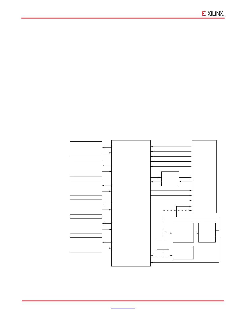
�The� XM104� provides� a� number� of� connectors� which� break� out� the� FPGA� multi-gigabit�
�transceiver� (MGT)� interface� signals� to� and� from� the� board� interface.� Figure� 1-2� shows� a�
�block� diagram� of� the� XM104.� Each� MGT� data� port� interface� consists� of� two� differential�
�pairs� of� MGT� signals,� one� pair� for� the� transmitter� and� one� pair� for� the� receiver.� MGT� Data�
�Ports� 0� and� 1� are� each� wired� to� four� SMA� connectors.� MGT� Data� Ports� 2� and� 3� are� each�
�wired� to� host� Serial� ATA� connectors� J11� and� J12� respectively.� MGT� Data� Ports� 4� through� 7�
�are� wired� to� a� 10GE� Base-CX4� connector� supporting� a� XAUI� application� interface.� MGT�
�transmitter� Data� Ports� 8� and� 9� are� electrically� looped� back� to� the� board� receiver� ports� 8� and�
�9� respectively.� The� ML605� does� not� support� Data� Port� 8� and� 9� interfaces.�
�Silicon� Laboratories� Si570� serial� IIC� bus� reprogrammable� LVDS� clock� source� and� a� Si5368�
�any-rate� precision� clock� multiplier� and� jitter� attenuator� integrated� circuits� provide� a�
�variety� of� programmable� differential� clock� sources� to� the� board’s� FGPA.� The� Si5368�
�integrated� circuit� receives� three� differential� LVDS� clock� inputs� from� the� board� and� outputs�
�five� LVDS� differential� clock� outputs� to� the� FPGA.�
�A� 2� Kb� serial� IIC� EEPROM� is� also� connected� to� the� IIC� interface� of� the� board� providing�
�non-volatile� storage.� The� serial� IIC� interface� also� connects� to� the� Si570� and� Si5368�
�integrated� circuits� enabling� the� board’s� FPGA� to� program� the� clock� circuitry� on� the� XM104.�
�X-Ref� Target� -� Figure� 1-2�
�J1� FMC� HPC� Interf� a� ce�
�S� i5� 3� 68�
�MGT� D� a� t� a� Port� 0�
�S� MA� (4x)�
�J� 3� ,� J4,� J5,� J6�
�MGT� D� a� t� a� Port� 1�
�S� MA� (4x)�
�DP0�
�DP1�
�GBTCLK0_M2C�
�CLK0_M2C�
�CLK1_M2C�
�CLK2_M2C�
�CLK� 3� _M2C�
�CKOUT1�
�F� S� _OUT�
�CKOUT2�
�CKOUT� 3�
�CKOUT4�
�J7,� J8,� J9,� J10�
�Level�
�S� hifter�
�Any-r� a� te� Clock�
�MGT� D� a� t� a� Port� 2�
�S� eri� a� l� ATA� J11�
�MGT� D� a� t� a� Port� 3�
�S� eri� a� l� ATA� J12�
�DP2�
�DP� 3�
�LA00_CC�
�LA01_CC�
�LA17_CC�
�CKIN1�
�CKIN� 3�
�CKIN4�
�CKIN2�
�S� i570�
�MGT� D� a� t� a� Port� s� 4-7�
�10GE� B� as� e-CX4� J2�
�MGT� D� a� t� a� Port� s� 8-9�
�Electric� a� l� Loop� ba� ck�
�DP4-DP7�
�DP8-DP9�
�IIC�
�S� witch�
�Clock�
�156.25� MHz�
�Clock�
�Driver�
�2� K� b�
�IIC�
�EEPROM�
�GBTCLK1_M2C�
�UG5� 3� 6_02_120� 3� 09�
�Figure� 1-2:�
�XM104� Block� Diagram�
�10�
��FMC� XM104� Connectivity� Card� User� Guide�
�UG536� (v1.1)� September� 24,� 2010�
�发布紧急采购,3分钟左右您将得到回复。
相关PDF资料
HW-PC4-MS
CABLE MOUSE SPLITTER FOR HW-PC4
HW-S3PCIE-DK-PROMO1
KIT STARTER SPARTAN3 PCI EXPRESS
HW-SPAR3-SK-UNI-G
KIT STARTER SPARTAN-3
HW-SPAR3E-DISP-DK-UNI-G
KIT DEV SPARTAN3E DISPLAY
HW-SPAR3E-SK-UK-G
KIT STARTER SPARTAN-3E
HW-USB-II-G
PLATFORM CABLE USB II
HW-USBN-2A
ACCY USB DOWNLOAD CABLE STD SPD
HW-V4-ML401-USA
EVALUATION PLATFORM VIRTEX-4
相关代理商/技术参数
HW-FMC-XM105-G
功能描述:FMC XM105 CONNECTIVITY CARD RoHS:是 类别:编程器,开发系统 >> 配件 系列:* 产品培训模块:Lead (SnPb) Finish for COTS
Obsolescence Mitigation Program RoHS指令信息:IButton RoHS Compliance Plan 标准包装:1 系列:- 附件类型:USB 至 1-Wire? RJ11 适配器 适用于相关产品:1-Wire? 设备 产品目录页面:1429 (CN2011-ZH PDF)
HW-FPGABOARD
制造商:Xilinx 功能描述:FPGA DEMONSTRATION BOARD
HWFR-B310
制造商:LUMILEDS 制造商全称:LUMILEDS 功能描述:Lumileds P3 Series TS AlInGaP Chips
HWFR-B310101
制造商:LUMILEDS 制造商全称:LUMILEDS 功能描述:Lumileds P3 Series TS AlInGaP Chips
HWFR-B310102
制造商:LUMILEDS 制造商全称:LUMILEDS 功能描述:Lumileds P3 Series TS AlInGaP Chips
HWFR-B310112
制造商:LUMILEDS 制造商全称:LUMILEDS 功能描述:Lumileds P3 Series TS AlInGaP Chips
HWFR-B317
制造商:LUMILEDS 制造商全称:LUMILEDS 功能描述:Lumileds P4 Series LED Chips
HWFR-B410
制造商:LUMILEDS 制造商全称:LUMILEDS 功能描述:Lumileds P3 Series TS AlInGaP Chips